
Author: Dr. Changwook Han, Principal Analyst
Editor: Choong Hoon Yi, CEO, Chief Analyst
BOE has outlined a direction to transform from a display-panel-centered business structure into an ‘Optoelectronics Integration’ company encompassing semiconductor packaging and optical interconnects. Rather than simply expanding its existing LCD and OLED production capabilities, the strategy is to extend its glass-substrate and thin-film/microfabrication technologies into new industrial domains.
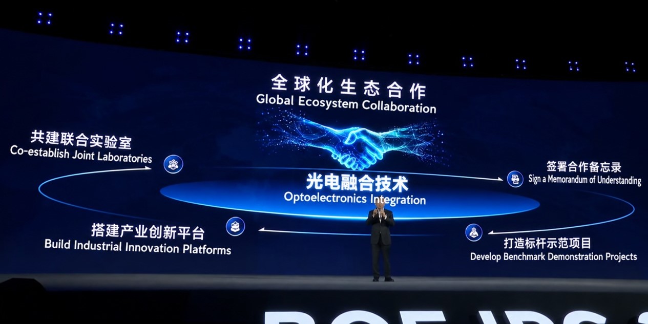
BOE’s strategy to expand the global collaborative ecosystem based on optoelectronics integration, presented at IPC 2026 (Source: BOE IPC 2026 presentation video)
At IPC (Innovation Partner Conference, BOE’s Global Innovation Partner Conference), BOE described its growth trajectory as a series of successive growth curves extending from TFT-LCD to OLED, IoT, and smart devices. IPC is BOE’s flagship innovation event where the company shares its mid- to long-term technology directions and new business strategies with technology and industry partners. Under a strategy of securing the next growth axis before a technology or market reaches maturity, BOE presented Glass-based Perovskite, Glass-based Packaging, and Optical Interconnect as next-generation growth areas at this year’s event.
Most notable is BOE’s attempt to carry the manufacturing foundation it has accumulated in the display industry directly into new businesses. Experience in handling large-area glass substrates, thin-film deposition, fine patterning, and mass production is a core asset BOE has built over many years of display manufacturing. BOE is seeking to extend these process capabilities beyond panel manufacturing into the optoelectronics and semiconductor fields.
Glass-based Packaging is a representative example of this strategy. As the performance of semiconductors for AI and HPC increases, the importance of inter-chip interconnect density and large-area packaging is growing. BOE identified advanced packaging using a Glass Core, rather than conventional organic-substrate-centered packaging structures, as a new business opportunity. This can be seen as an approach that connects its experience in manufacturing large glass substrates for displays to semiconductor packaging.
Optical Interconnect follows the same trajectory. In AI data centers, the rapid increase in computing workloads and data traffic is increasingly highlighting the power consumption and bandwidth limitations of electrical interconnects. BOE’s inclusion of Optical Interconnect as a next-generation growth technology can be interpreted as a move to expand the competitive arena from ‘technology for making screens’ to ‘technology for processing, transmitting, and displaying information using light.’
The change revealed by this presentation differs in nature from simply adding new businesses. In the past, shifting the center of display technology from LCD to OLED was at the core of its growth strategy; going forward, BOE’s direction of using the Glass and thin-film process capabilities acquired through display manufacturing themselves as a technology platform is becoming clearer.
Ultimately, the next growth curve presented by BOE is an expansion of its business boundaries from Display to Advanced Packaging and Optical Interconnect. Going forward, in evaluating BOE’s competitiveness, a key point to watch will be not only its LCD and OLED production capacity and panel shipments, but also how far these new glass-substrate-based businesses translate into actual mass production and customer acquisition.