
Canon Tokki Develops RGB Evaporation System for 12-inch Si Wafers, Achieving ±0.04 μm Alignment Accuracy
Canon Tokki has unveiled a high-resolution evaporation system for 12-inch Si wafers aimed at direct RGB patterning of OLEDoS (micro OLED). At the 43rd Organic EL Symposium held in Fukuoka, Japan, on November 12–13, the company presented the configuration and evaluation results of a prototype experimental system that raises wafer-to-mask alignment accuracy to ±0.1 μm or better.
(Image: 43rd Organic EL Symposium presentation, Canon Tokki)
Si wafer-based micro OLEDs are small panels of 0.5–2 inches used in AR/VR devices and camera electronic viewfinders (EVFs). Because they are viewed close to the eye, they require resolutions of 3,000 ppi or higher. At such resolutions it is difficult to pattern separate RGB subpixels by mask evaporation, so the WOLED approach, which places color filters on top of a white OLED, has been adopted; however, the color filters lower luminous efficiency. According to the presentation, the alignment accuracy of evaporation systems for OLED mass production is about ±3 μm on G6H glass substrates, while that of WOLED evaporation systems for micro OLED is at the ±10–100 μm level.
Canon Tokki developed a magnetic levitation stage, an IR camera, a mask tilt-tracking mechanism, and a micro-contact alignment mechanism. The magnetic levitation stage holds the wafer with an electrostatic chuck and controls its position by magnetic levitation. Taking advantage of the fact that Si wafers transmit infrared light, the IR camera detects alignment marks from the back side of the wafer.
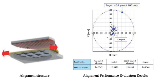
Because micro OLED masks have openings only a few μm wide, even a slight gap between the mask and the wafer causes shadowing. Making the mask thinner reduces its strength and risks breakage on contact, and since the wafer hardly deforms, uniform close contact is also difficult to achieve. Canon Tokki therefore tracks and corrects the position and tilt of the wafer and mask before contact, then aligns them through fine lateral movements of a few μm while the two are in light contact.
In the evaluation, alignment accuracy (3σ) was ±0.0347 μm in the non-contact state and ±0.0368 μm in the final state with the mask clamped by magnets. Although accuracy decreased slightly after magnetic clamping, the value is well below the ±0.1 μm target.
A distinctive feature of the system configuration is a dedicated mask transfer system, with masks exchanged by a robot from the rear of the evaporation chamber. In conventional systems, wafers and masks share the same transfer system, and organic material deposited on the mask after evaporation becomes a source of particles. Separating the transfer systems reduces the risk of wafer contamination, and a mask stock chamber and cleaning unit can be connected to the cluster-type exchange section. In high-resolution RGB evaporation, film accumulated on the mask affects shadowing characteristics, making periodic mask replacement essential, so this structure is advantageous for mass-production operation.
Noh Chang-ho, UBI Research