
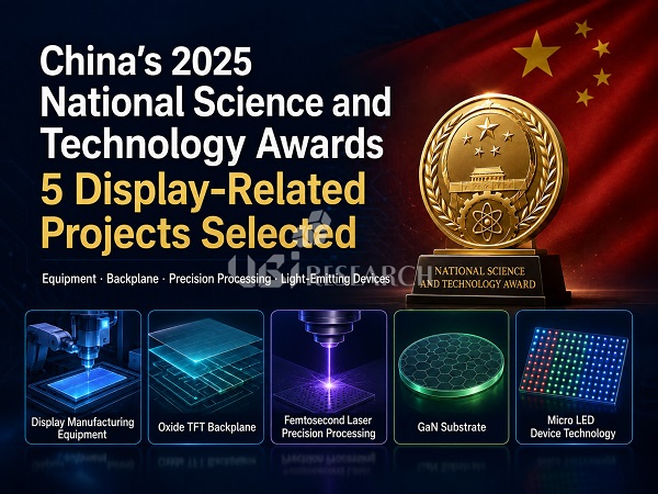
Image illustrating five display-related projects in China’s 2025 National Science and Technology Awards (Created with ChatGPT)
At the awards ceremony held in Beijing on July 8 2026 for China’s 2025 National Science and Technology Awards (国家科学技术奖), key display companies including BOE (京东方) and Visionox (维信诺) were honored among the winners. The ceremony recognized a total of 258 projects and 11 science and technology experts.
UBI Research’s analysis of the published award list identified five projects directly related to the display sector: three projects concerning manufacturing equipment, backplanes, and OLED precision processing, and two projects on light-emitting device base technologies that are extendable to LED and Micro LED. This reflects how China’s technology development focus is expanding beyond simply increasing panel production capacity to encompass core equipment, TFT backplanes, ultra-precision processing, and compound semiconductor substrates and device structures.
National Science and Technology Progress Award, Second Class: Localization and Industrialization of High-Resolution, Large-Area Display Manufacturing Equipment (Shanghai University, Shanghai Micro Electronics Equipment Group (SMEE), Hefei Xinyihua Intelligent Machine, BOE, Tianma, Kunshan Govisionox Optoelectronics, SeeYA Technology)
The project “Core Technologies, Equipment, and Industrialization for High-Resolution, Large-Area Manufacturing of New-Type Displays” is recognized as an industrialization achievement in which equipment makers and panel makers jointly developed core processes and manufacturing equipment and applied them to actual production lines. It illustrates how the competitive axis of China’s display industry is shifting from panel production capacity toward the localization of exposure, patterning, and automation equipment and the internalization of process technology. BOE, Tianma, and Visionox-affiliated companies participated alongside SeeYA, reinforcing a supply-chain foundation that can extend beyond LCD to OLED and next-generation display manufacturing technologies.
National Science and Technology Progress Award, Second Class: Core Backplane Technology for Oxide Semiconductors, IT OLEDs, and High-Resolution Displays (BOE, Chengdu BOE Display Technology, Sun Yat-sen University, Tsinghua University, Shanghai Jiao Tong University, Peking University, Institute of Microelectronics of the Chinese Academy of Sciences)
The project “Research and Industrial Application of Advanced Oxide Semiconductor Technology for Smart Displays” is characterized by an industry-academia-research structure combining the materials and device research capabilities of universities and national research institutes with BOE’s process and mass-production capabilities. Oxide semiconductors, with their high electron mobility, low leakage current, and large-area uniformity, are emerging as core TFT backplane technology not only for LCD but also for IT OLEDs used in laptops, tablets, and monitors. In particular, as uniformity, yield, and investment efficiency for large-area substrates become increasingly important in 8.6-generation IT OLED, the strategic value of oxide TFT is expected to grow further.
National Technology Invention Award, Second Class: Femtosecond Laser Precision Cutting and Micro-Hole Processing for Flexible OLED (Beijing Institute of Technology, Shenzhen Han’s Semiconductor Equipment Technology, the 707th Research Institute of China State Shipbuilding Corporation, Guangzhou Govisionox Technology, a Visionox affiliate)
The project “Femtosecond Laser Electron Dynamic Control Micro-Processing Technology and Applications” is an ultra-precision laser processing technology that reduces material damage by controlling electron behavior and energy transfer during processing using ultra-short pulses on the order of 10⁻¹⁵ seconds. This technology has been applied to the precision cutting of flexible OLED modules and to micro-hole processing for camera and sensor openings, and is credited with contributing to ultra-slim bezel implementation as well as improvements in processing quality and mass-production yield. The participating institutions stated that the technology has already been applied in mass production for several mainstream end products. This shows that China’s localization of display equipment is expanding to include ultra-precision processing in back-end OLED module processes.
National Technology Invention Award, Second Class: Core Substrates for GaN Light-Emitting Devices, Securing Micro LED Performance and Yield (Peking University, Dongguan Zhongjia Semiconductor, Guangdong Zhongtu Semiconductor, NAURA, Songshan Lake Materials Laboratory)
The project “Core Substrate Technology for GaN-Based Light-Emitting Devices” achieved as its main result a stable manufacturing foundation for high-efficiency, high-reliability GaN light-emitting devices by improving crystal quality, wavelength uniformity, luminous efficiency, and production yield of GaN substrates. As chip sizes shrink, the impact of wafer defects and characteristic variation grows, making the importance of high-quality substrates and epitaxy-based technology correspondingly greater.
National Natural Science Award, First Class: V-Defect Three-Dimensional PN Junction, Base Technology for High-Efficiency Micro LED Devices (Nanchang University)
The project “V-Defect Three-Dimensional PN Junction and Applications” is basic research conducted by Nanchang University. The three-dimensional PN junction structure using V-defects can improve current injection and electron-hole recombination characteristics in nitride-based LEDs, giving it potential for extension to high-efficiency LED and Micro LED device structures.
China’s Display Technology Policy Expanding into Equipment, Backplanes, Precision Processing, and Light-Emitting Devices
UBI Research assesses that these award results serve as an indicator of the direction of China’s display industry technology development. BOE participated in both the high-resolution/large-area manufacturing equipment project and the oxide semiconductor project, confirming its central role in China’s display technology development and industrialization. The participation of equipment companies such as SMEE, Xinyihua, and NAURA also shows that China is broadening the scope of supply-chain self-sufficiency beyond panel production to include core equipment. Awards were concentrated on domestic-substitution technology projects in which private companies with market dominance reduced dependence on foreign technology through industry-academia cooperation, even in the display sector — suggesting that the self-sufficiency of China’s display value chain is approaching completion across the entire spectrum, from basic theory and core technology to mass production and equipment.
Changho Noh, Senior Analyst at UBI Research (chnoh@ubiresearch.com)
▶2026 Analysis Report on China’s OLED Supply Chain Management
▶China Display Industry Trends Report
※ This article is produced by UBIResearchNet.
Unauthorized reproduction or citation without source attribution is prohibited.
When quoting, please clearly indicate the source (UBIResearchNet) and provide a link.