
Development of technologies that form OLED pixels without an FMM (Fine Metal Mask) is spreading across Korean and Chinese panel makers. With the FMM process, an expensive new mask must be fabricated every time the panel size or resolution changes, and as substrates grow larger, mask sagging and alignment errors make scale-up difficult. The wide non-emitting area also limits how far the aperture ratio can be raised. Forming pixels by photolithography or inkjet printing can ease these constraints and substantially increase the aperture ratio, which is why these approaches are drawing attention as next-generation process candidates for the Gen 8.6 IT OLED era.
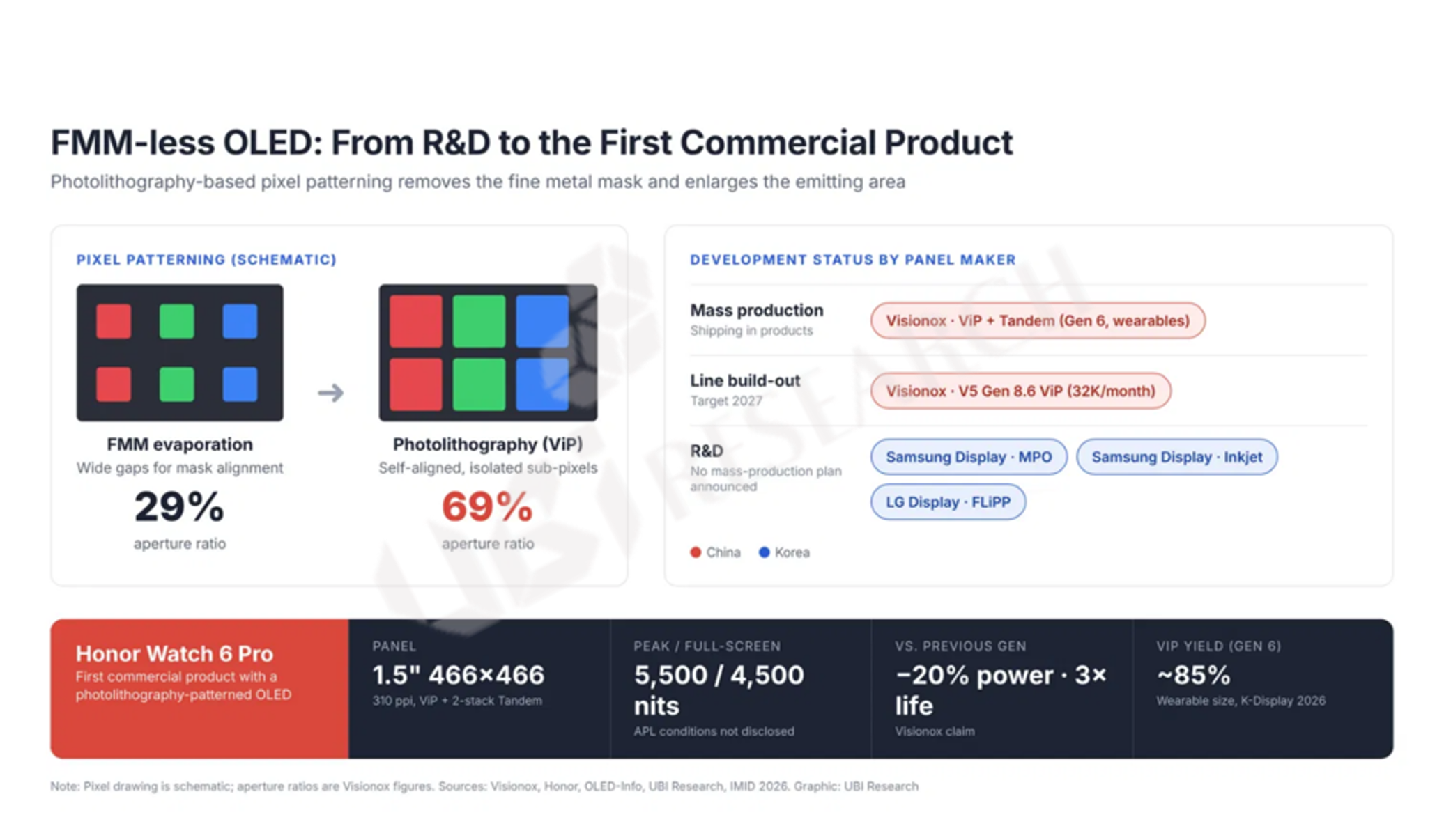
The image compares the aperture ratio of conventional FMM and Visionox ViP and summarizes FMM-less OLED development status across major panel makers. ViP raises the aperture ratio from 29% to 69%, while Visionox has moved into commercial production and Samsung Display and LG Display remain in the R&D stage.
Korean panel makers are also accelerating development. Samsung Display has been researching its in-house photo-patterning technology, MPO (Micro Patterned OLED), as well as inkjet OLED, and is reported to have recently stepped up its development efforts. LG Display unveiled FLiPP, based on photo patterning, for the first time at IMID 2026 in August. However, both companies remain at the R&D stage, and neither has formalized mass-production investment or a specific commercialization schedule.
At present, Visionox (维信诺) is the only company to have applied FMM-less OLED to a mass-production product. Visionox supplied Honor (荣耀) with a panel for its ‘Watch 6 Pro’ smartwatch that combines a tandem structure with ViP (Visionox intelligent Pixelization), the proprietary photolithography technology it unveiled in May 2023. The 1.5-inch (466×466, 310 ppi) panel delivers a peak luminance of 5,500 nits and a full-screen luminance of 4,500 nits, and Visionox stated that it has reduced power consumption by 20% and tripled lifetime compared with the previous generation. When Visionox announced ‘Q1 mass-production shipments for Honor wearables’ in April, it did not disclose the product name; that result has now reached the market as the Watch 6 Pro. Honor has also promoted the panel as a ‘pixel lithography screen.’
ViP’s strengths grow when it is combined with tandem structures. In the FMM process, the number of emitting-layer deposition and mask-alignment steps increases as stacks are added, whereas ViP can accommodate additional stacks simply by adding deposition chambers. The aperture ratio also rises from 29% to 69%, allowing a lower current density at the same luminance. In its keynote at SID 2026, Visionox stated that, at 800 nits, ViP can reduce power consumption by 6% for a 7.9-inch panel and by 20% for a 14.2-inch panel, emphasizing that the benefit of reduced cathode resistance grows as panels get larger.
The significance of this product lies less in its luminance record than in the fact that a panel made with an FMM-less process has passed the reliability standards of a mass-production product.
The remaining challenges are yield and scale-up. At K-Display 2026, Visionox stated that wearable ViP yield on its G6 line had reached about 85%, but yields at panel sizes larger than smartphones are reported to be considerably lower than with the FMM process. ViP panels are reportedly being produced in small volumes on the G6 line, targeting around 3 million units per year combined for wearables and smartphones, and ViP panels for Xiaomi (小米) watches, smartphones, and smart glasses are also said to be in development. Phase 1 of the mass-production Hefei G8.6 V5 line (32K sheets/month) has a capacity of 8K sheets/month and targets mass production in 2027. Vertical evaporators from AKT, an AMAT (Applied Materials) affiliate, have been installed for Phase 1. Because IT panels are planned to be produced with a 2-stack tandem structure, the effective capacity per evaporator will be about half that of a single-stack structure. How uniformity of the photo process and damage to organic layers are managed on large-area substrates will be the key variables for yield.
Watches, with their small panel area, are the market where the yield risk of a new process is lowest. The real competitiveness of FMM-less technology depends on whether yield and cost can be secured at smartphone and IT sizes, and the operating results of Visionox’s V5 line in 2027 are expected to be the first real test.