
As data traffic in AI infrastructure increases, Micro-LEDs are gaining attention as devices for transmitting optical signals between chips and servers. The key to optical signal transmission is a “wide-and-slow” parallel architecture that distributes data across hundreds to thousands of channels. This architecture increases aggregate bandwidth while reducing the speed required of each channel and the power consumed by complex signal processing and compensation circuits. CPO (Co-Packaged Optics) places optical engines in the same package as computing or switching chips.
United States Expands Customer Evaluation and System Validation
Avicena announced that it began supplying LightBundle 1 Tbps evaluation kits to customers and partners in August 2026. The kits deliver an aggregate data rate of approximately 1 Tbps by operating up to 335 channels at 3 Gbps each. At MicroLED Connect in September, the company introduced fiber bundles supporting distances of up to 5 m, along with error detection and link energy evaluation capabilities.
Microsoft Research’s Cambridge team in the United Kingdom presented a prototype with 100 channels operating at 2 Gbps each in its Mosaic paper at SIGCOMM 2025. In 2026, it announced an AOC (Active Optical Cable) proof of concept in collaboration with MediaTek. The design integrates logic, drivers, and receiver amplifiers on a single CMOS chip, with Micro-LEDs and photodetectors directly bonded to it.
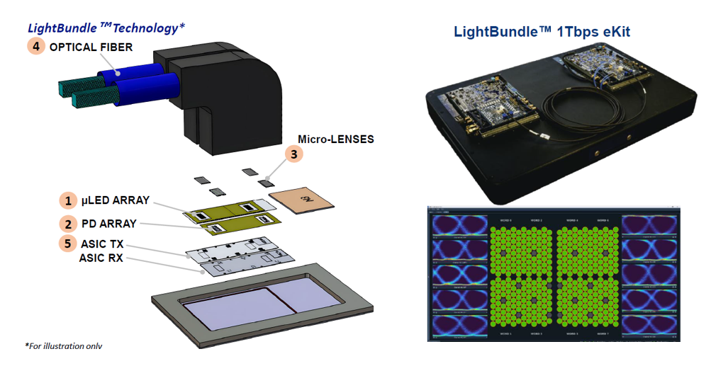
Avicena’s LightBundle™ Technology and 1 Tbps evaluation kit. (Source: Avicena, MicroLED Connect 2026)
■ Taiwan Combines Light Sources with Receiver and Packaging Technologies
At SEMICON Taiwan 2026, AUO unveiled a system-level module targeting a transmission distance of 10 m. Ennostar supplies the transmitting light sources, while Tyntek provides the receiver devices. AUO integrates mass transfer, RDL packaging, optical coupling, and system design. The module uses Corning optical fibers, and Daxin’s photosensitive dielectric material is applied to the RDL (Redistribution Layer) structure.
In January 2026, PlayNitride and Brillink announced joint development combining green Micro-LEDs with GeSi avalanche photodetectors (APDs). The approach uses Brillink’s meta-optics and vertical optical coupling of two-dimensional arrays to improve alignment accuracy and receiver sensitivity.
■ China Expands Device Development and Industry–University Collaboration
BOE HC SemiTek and Nanjing University established a joint Micro-LED CPO laboratory on August 25, 2026. The collaboration combines HC SemiTek’s epitaxy, chip manufacturing, and mass production capabilities with Nanjing University’s research into wide-bandgap semiconductors to develop core technologies, including optical interconnects and integrated circuits. In March, Sanan announced that it had developed high-speed modulated Micro-LED light sources with Tsinghua University and China Mobile.
■ Future Opportunities in Technology and Industry
The technical opportunity for Micro-LED optical interconnects lies in achieving sufficient modulation speed and optical output at low drive currents. Epitaxial designs that control recombination characteristics in the light-emitting layers, together with efficiency improvements in microscopic devices, provide a basis for increasing transmission speeds while reducing power consumption and heat generation. Device structures that control emission direction, microlenses, and highly sensitive receivers can further compensate for coupling losses and improve link power efficiency.
Direct bonding of light-source and receiver arrays to CMOS is also expected to become increasingly important. It enables the integration of many optical channels while keeping electrical connections short. This could broaden the use of precision transfer and bonding, optical alignment, and simultaneous testing of multiple channels.
From an industry perspective, opportunities are emerging to extend Micro-LED manufacturing technologies developed for displays into components and processes for AI infrastructure. LED manufacturers could expand into epitaxy for communications and high-speed emitting arrays, while display and packaging companies could broaden their businesses into mass transfer and heterogeneous integration modules. Suppliers of optical components, fibers, connectors, and test equipment may also see demand for development supporting high-density parallel connections.
Initial applications are expected to emerge in short-reach connections within and between racks, where existing server interfaces can be used. Once package-level yield, thermal stability, and maintenance requirements have been validated, applications could expand to NPO (Near-Packaged Optics) and CPO, which place optical engines closer to computing chips. Collaboration linking communications circuits with optical and packaging technologies is expected to form a new supply chain for the Micro-LED industry.