
Simultaneous transfer and bonding, fluidic self-assembly and slot-die-coating-based transfer were presented in succession on the second day of MicroLED Connect 2026.
Reporting & Analysis: UBI Research
Editor: Choonghoon YI, CEO & Chief Analyst
The afternoon program at MicroLED Connect 2026 covered three approaches to scaling MicroLED transfer and bonding in consecutive sessions on September 17. The presentations ran from 1:10 p.m. to 1:50 p.m. local time in Eindhoven, the Netherlands, corresponding to 8:10 p.m. to 8:50 p.m. in Korea.
ETRI presented ‘From Materials to OSAT: SITRAB Technology for Scalable Micro-LED Transfer and Bonding.’ The title positioned transfer and bonding technology spanning the materials stage through back-end processing as a single route to scale-up.
A related paper published by ETRI researchers in 2026 explains that MicroLEDs were transferred and bonded to a display substrate within seconds using laser-induced soldering. The SITRAB adhesive retained its soldering function after repeated infrared-laser irradiation and was used to sequentially integrate different MicroLEDs onto the same backplane.
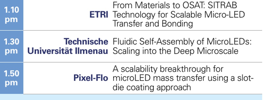
Official September 17 schedule showing consecutive transfer and bonding presentations by ETRI, TU Ilmenau and Pixel-Flo. Source: MicroLED Connect official handout
TU Ilmenau then presented ‘Fluidic Self-Assembly of MicroLEDs: Scaling into the Deep Microscale.’ The official agenda identified the extension of fluidic self-assembly to smaller MicroLED dimensions as the subject of the presentation.
Pixel-Flo presented ‘A scalability breakthrough for microLED mass transfer using a slot-die coating approach.’ The organizer introduced the session as an examination of mass-transfer scalability using slot-die coating.
The three presentations did not repeat the same process. They placed three different approaches in the same time block: integrated transfer and bonding, fluidic self-assembly, and coating-based mass transfer. The official agenda did not include quantitative figures for throughput, yield or substrate size for any of the approaches.
The same day’s program also included sessions on 300 mm GaN-on-Si, large-area nanoimprint and MicroLED testing. The program positioned transfer technology as one part of mass production alongside epitaxy and substrates, patterning, and testing.
The organizer said presentation recordings and slides would be available on the event platform about one week later. Process conditions and quantitative performance for each approach can be confirmed after the full presentation materials are released.
Source: MicroLED Connect official event page · TechBlick official agenda announcement, June 30, 2026 · ETRI published research materials · Microsystems & Nanoengineering paper, 2026