
China-based StarkSemi has established an 8-inch Si-GaN MicroLED production system and is extending its technology from monochrome microdisplays to vertically stacked full-color devices. At CIOE 2026, the company presented a manufacturing-platform strategy linking wafer, bonding, and stacking processes.
Written by: Dr. Namdeok Kim, Senior Analyst
Editor: Dr. Choonghoon YI, CEO & Chief Analyst
China-based StarkSemi is building a MicroLED mass-production platform centered on 8-inch silicon-based GaN (GaN-on-Si), while expanding into AR microdisplays and optical interconnects for AI data centers. At CIOE 2026, held on September 9, 2026, the company displayed not only monochrome MicroLED products but also 8-inch GaN epitaxial wafers, Chip-on-Wafer (CoW) processed wafers, hybrid-bonding samples, and process wafers for vertically stacked single-chip full-color devices. Rather than emphasizing finished displays, the company highlighted an integrated manufacturing system spanning epitaxy, devices, bonding, and heterogeneous integration.
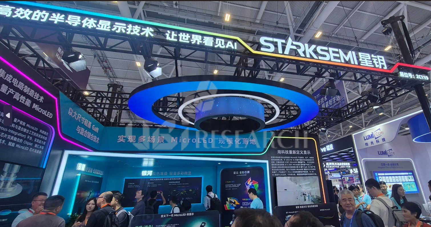
StarkSemi booth at CIOE 2026 (Photo: UBI Research)
8-inch End-to-End Process Established as Monochrome MicroLED Enters Mass Production
StarkSemi established a pilot line for the full 8-inch Si-GaN MicroLED process in September 2025. The company’s announced plan calls for annual capacity of approximately 12,000 wafers. Its IDM structure connects GaN epitaxial growth, chip fabrication, and wafer bonding through in-house processes. The company currently operates pilot mass-production lines for 8-inch InGaN and AlInGaP and is also pursuing 8- and 12-inch production lines.
At CIOE 2026, StarkSemi demonstrated this strategy through actual process wafers. The exhibit included large-diameter Si-GaN epitaxial wafers, CoW processed wafers, hybrid-bonding samples, and intermediate process wafers designed to vertically integrate R/G/B emissive layers with CMOS. A company representative described the process chain from large-diameter Si-GaN epitaxy through CoW and precision hybrid bonding to vertically stacked single-chip full color as the centerpiece of the exhibit. The company says its monochrome MicroLED chips have already entered mass production. Two-color and three-color integrated products, however, are not yet in mass production. Samples of both types have been supplied to customers for product adoption and validation.
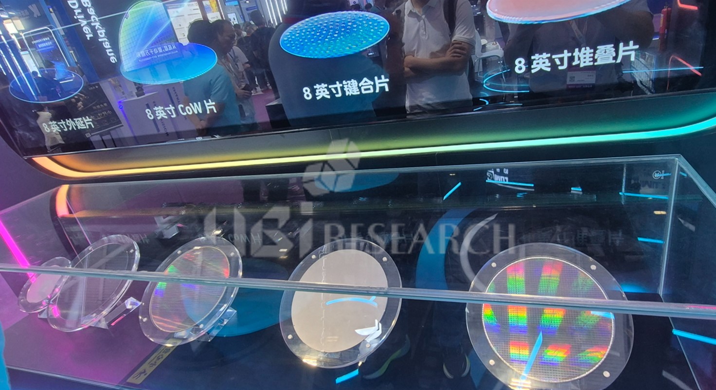
8-inch process samples displayed by StarkSemi (Photo: UBI Research)
Multi-Wavelength MicroLED Beyond Standard Green
CIOE 2026 also showed StarkSemi’s strategy of tuning MicroLED emission wavelengths to customer optical systems. The company exhibited multi-wavelength monochrome MicroLED microdisplays, including 490 nm and 580 nm devices. Instead of offering only conventional green MicroLEDs, StarkSemi adjusts the emission wavelength through its in-house Si-GaN epitaxial process to address the requirements of different waveguides and optical systems.
The company’s official monochrome MicroLED portfolio covers 0.10-, 0.12-, and 0.13-inch devices with resolutions from 500 × 380 to 800 × 600 and pixel pitches of 2.5 to 4 μm. The CIOE exhibit also introduced a 530 nm monochrome product and the availability of multiple wavelength options. This multi-wavelength strategy is relevant to AR MicroLED applications. Because waveguide diffraction efficiency and optical loss vary by wavelength, jointly optimizing the optical system and emission wavelength can increase design flexibility.
From Two-Color Stacking to Vertical R/G/B+CMOS Integration
For full-color operation, StarkSemi’s longer-term direction is vertical stacking using hybrid bonding. At CIOE, the company displayed a two-color sample with vertically integrated green and red emissive layers. According to the company, each layer can be driven independently to change the output color. This two-color structure serves both as an intermediate product between monochrome and full RGB and as a platform for validating the bonding and back-end yields required for future R/G/B+CMOS vertical integration. The company ultimately aims to build a single-chip full-color architecture that vertically stacks R/G/B emissive layers and CMOS within the next several years.
MicroLED Competition Expands from Devices to Wafer Manufacturing Platforms
The central message from StarkSemi at CIOE 2026 was not the performance of any single MicroLED product, but a strategy to connect epitaxy, device fabrication, hybrid bonding, and vertical stacking within one 8-inch wafer-based manufacturing system. As pixel pitches for AR MicroLEDs shrink to several micrometers, competitiveness is not determined by the peak brightness of individual LEDs alone. Wavelength and luminance uniformity across the wafer, efficiency at very small pixel sizes, defect density, CMOS alignment and bonding yield, and cumulative yield after RGB stacking all determine mass-production viability. StarkSemi is seeking to address these requirements through 8-inch semiconductor-wafer processing and heterogeneous integration rather than conventional small-LED manufacturing methods.
The simultaneous display of monochrome products, epitaxial wafers, CoW wafers, hybrid-bonding samples, and RGB stacking process wafers at CIOE clearly illustrated the company’s direction. Monochrome MicroLEDs have already entered mass production. Key indicators for future competitiveness will be customer validation and yield for two-color and RGB vertical stacks, together with the ability to reproduce those results reliably on large-area 8-inch wafers.
Sources: StarkSemi official materials and UBI Research coverage at CIOE 2026