
1. Chip Miniaturization and Efficiency Loss
Reducing micro-LED chip size serves two objectives: achieving higher resolution and increasing the number of chips per wafer to lower chip costs. The challenge is that efficiency tends to decline as chips become smaller. This report examines the causes of these losses, the technologies developed to mitigate them, and how companies are applying these approaches.
The decline in efficiency as chips shrink is largely associated with their sidewalls. Etching creates defects on chip sidewalls, and as chip dimensions decrease, the perimeter-to-area ratio rises, increasing the influence of these defects. Nonradiative recombination at these sites can be particularly pronounced at low current.
Smaller chips may have reduced electrode contact areas, increasing contact resistance. This can raise the driving voltage and lower wall-plug efficiency (WPE). In addition, a larger proportion of light may exit through the sidewalls, broadening the angular emission distribution and reducing usable light in optical systems that collect primarily forward-emitted light.
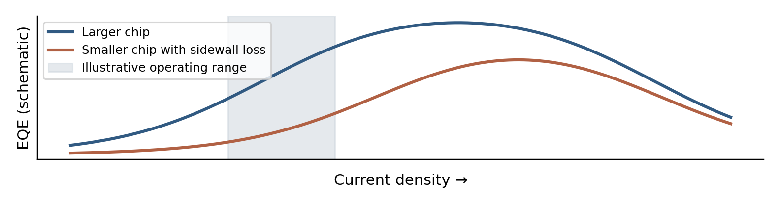
Figure 1. Changes in EQE with Chip Size (Schematic)
Metric | Definition | Conditions to Report |
EQE (External Quantum Efficiency) | Ratio of photons emitted externally to electrons injected | Peak value or value at a specified current density |
WPE (Wall-Plug Efficiency) | Ratio of optical output power to input electrical power | Driving voltage, current, and measured optical output power |
Efficiency values for the same device differ depending on the metric used, so the metric needs to be specified. EQE measures the ratio of externally emitted photons to injected electrons, whereas WPE also accounts for electrical losses associated with the driving voltage.
2. Efficiency and Color Stability of Red Devices
Red devices are known to suffer a greater efficiency decline with miniaturization than blue and green devices. AlGaInP, commonly used for red emitters, has a higher surface recombination velocity than InGaN, and its carriers travel farther within the emitting layer. Consequently, even carriers injected into the interior can reach the sidewalls and recombine without emitting light. In blue and green InGaN, by contrast, carriers can become localized in regions of nonuniform indium composition, making them less likely to reach the sidewalls and less susceptible to sidewall effects at the same chip size.
InGaN-based red emitters are therefore being developed, although they face a different set of challenges. The table below summarizes the differences between the two material systems.
Category | AlGaInP-Based Red | InGaN-Based Red |
Miniaturization-related losses | Recombination occurs at sidewalls, and carriers that migrate to the sidewalls also contribute. The magnitude of loss depends on etching and surface conditions. | In addition to sidewall losses, indium composition, crystal quality, strain, and carrier localization also play a role. |
Current-dependent changes | Defect-related recombination affects performance at low current, while losses and self-heating become influential at high current. | Wavelength may shift as internal electric fields are screened or available states become filled. |
Temperature-dependent changes | Carrier leakage and nonradiative recombination may increase, potentially shifting the wavelength. | Increasing nonradiative recombination and changes in carrier distribution alter efficiency and the spectrum. |
Producing red emission from InGaN requires a higher indium content, which increases crystal strain and the electric field within the quantum wells. This tends to reduce efficiency, while changes in current can also shift the emission wavelength. In a UCSB device, the wavelength shortened from 619 nm at turn-on to 589 nm at 150 A/cm². By comparison, raising the temperature from 30 °C to 200 °C produced a shift of approximately 7.5 nm. The direction of the shift also varies among devices; Ingantec has reported behavior in which the wavelength first shifted longer and then shorter.
A wavelength shift can change the displayed color, so InGaN red devices must be evaluated for color stability as well as efficiency. A narrow spectral linewidth under one measurement condition does not necessarily mean stable color across a wide current range. The extent of required color correction depends on the driving scheme and temperature. Driving compensation will be discussed in a subsequent installment.
3. Efficiency Improvement Technologies by Loss Mechanism
The following table organizes improvement technologies according to the loss mechanisms discussed above.
Loss mechanism | Applicable material/color | Improvement technology | Reported effect and scope of interpretation |
Sidewall defects | InGaN and AlGaInP | InGaN: low-damage etching (e.g., neutral beam), KOH/TMAH wet removal of etch damage, and ALD passivation. AlGaInP: ammonium sulfide treatment. | Reduces surface defects and leakage paths. |
Active layer and lateral diffusion | AlGaInP-based red | Control carrier transport using AlInP/GaInP quantum wells. | Reduces lateral electron spreading and sidewall recombination, limiting the shift in the efficiency curve as chips shrink. |
Strain and internal electric field | InGaN red | Strain-relieving underlayers and short-period superlattices; optimization of barrier growth temperature and cap layers. | Facilitates indium incorporation and reduces defects. |
Current injection and distribution | All materials | Contact and electrode design; current confinement. | Reduces losses associated with resistance, leakage, and localized injection. |
Light extraction and emission modes | All materials, including InGaN red | Sidewall DBRs (distributed Bragg reflectors), reflective layers (SiO₂/Ta₂O₅), and nanowire photonic crystals with controlled ALD thickness and arrangement. | Controls emission direction to improve extraction efficiency. Photonic crystals can also reduce wavelength shifts. |
Reported Improvements in Representative Studies
For 10 μm AlGaInP devices, ammonium sulfide treatment increased EQE relative to untreated devices by 120.6% at 5 A/cm² and 49.8% at 100 A/cm². The greater benefit at lower current is consistent with sidewall losses being especially prominent in the low-current regime.
Researchers at the University of Michigan formed photonic crystals using nanowires and achieved a peak EQE of approximately 12% (at 4 A/cm²) in red InGaN. The spectral linewidth was a narrow 5 nm at 617 nm, and the color coordinates remained nearly unchanged even when the current was varied by more than a factor of ten.
UCSB achieved peak EQE of 20.8% and WPE of 13.2% in a planar device with a sidewall distributed Bragg reflector (DBR) made of SiO₂/Ta₂O₅. The device maintained an EQE of approximately 10% even at 200 °C.
4. Corporate Approaches to Efficiency Improvement
Companies are pursuing three broad approaches: applying sidewall-treatment processes, developing red epitaxial structures directly, and changing the device architecture itself, as in nanowire-based devices.
Comptek: Supplying Sidewall-Treatment Processes and Equipment
Comptek developed its Kontrox process to reduce defects and leakage at mesa sidewalls. In 2024, the company disclosed a 200 mm pilot line combining this process with plasma-enhanced ALD. Rather than redesigning the chip, the approach adds a process step to an existing device, positioning Comptek as a supplier of processing technology and equipment rather than a chip manufacturer.
Ingantec: Extending Red Epitaxial Development to Wafers
In September 2026, Ingantec announced peak EQE exceeding 20% in approximately 5 μm planar red InGaN devices (at 4–5 A/cm² and around 620–625 nm). EQE remained at 5–8% when the current density was increased to 40–140 A/cm².
The epitaxial and strain-management technologies were developed in collaboration with UCSB, where the measurements were also conducted. Ingantec is now seeking foundry, driver-circuit, and packaging partners based on its 4-inch sapphire wafer platform.
Aledia: Reducing Size Dependence with Nanowire Structures
Aledia has chosen to grow nanowires on silicon wafers to limit efficiency degradation as chips shrink. The company reports that blue chips retain 40% EQE at sizes as small as 3.5 μm, although it has not disclosed the measurement current density. Production currently uses 8-inch wafers, with plans to expand to 12-inch wafers.
5. Display Demonstrations and Industrial Collaboration
The following cases concern the realization of small pixels in actual displays or manufacturing partnerships rather than direct improvements in efficiency. Brightness and pixel pitch are not evidence of efficiency; they are included only as indicators of the level of color-display implementation.
Case | Publicly disclosed details | Products and production |
JBD | Announced the Roadrunner platform with a 2.5 μm pixel pitch and a color projector. | Reported adoption in customer products, including RayNeo X3 Pro, in January 2026. |
Porotech | Reported improvements in linewidth, wavelength, and thermal characteristics of its porous-GaN-based red InGaN technology (SpectraCore). | Announced 8-inch platform collaboration with Foxconn, PSMC, and GIS. |
QSI and Raontech; KAIST and Inha University | Demonstrated a 1,700 PPI display by integrating AlInP/GaInP red devices on CMOS. | Joint industry–academic development involving compound-semiconductor and driver-SoC companies. |
6. Conclusion
Although efficiency losses associated with chip miniaturization arise largely at the sidewalls, a growing body of results shows that surface treatments and structural designs can mitigate them. Companies are also beginning to offer these treatments as equipment-compatible processes, making sidewall-loss reduction increasingly applicable to manufacturing lines.
Red devices, however, cannot be addressed through sidewall treatment alone, and their challenges differ by material. AlGaInP is strongly affected by sidewalls, making loss reduction increasingly difficult as chip size decreases. InGaN needs improvements in both efficiency and current-dependent color stability. Most reported advances in red efficiency remain at the individual-device or demonstration stage.
References
[1] Advanced technologies in InGaN micro-LED fabrication to mitigate the sidewall effect. Light: Science & Applications (2025). doi:10.1038/s41377-025-01751-y. Review article.
[2] In situ dry repair and passivation unlocks size-independent performance in III-nitride micro-LEDs. Nature Photonics (2026). doi:10.1038/s41566-026-01990-4. Research article.
[3] Lee et al. Wafer-Bonded AlGaInP Red LEDs with Suppressed S-Droop through Surface Sulfidation. ACS Applied Materials & Interfaces (2026). doi:10.1021/acsami.5c20576.
[4] Wu et al. High efficiency, high color purity red micro-light-emitting diodes. Light: Science & Applications 15, 133 (2026). doi:10.1038/s41377-026-02227-3.
[5] Chao et al. 20.8% Peak External Quantum Efficiency of Red (619 nm) InGaN/GaN MicroLEDs. ACS Photonics (2026). doi:10.1021/acsphotonics.6c01611. Bibliographic details and official UCSB research coverage verified.
[6] Park et al. A monolithic three-dimensional integrated red micro-LED display on silicon using AlInP/GaInP epilayers. Nature Electronics 9, 170–179 (2026). doi:10.1038/s41928-025-01546-4.
[7] Comptek Solutions. Mesa sidewalls; Cleanroom and equipment capabilities. Official company materials. www.comptek-solutions.com/applications/mesa-sidewalls
[8] Ingantec. Ingantec Unveils 20% EQE, 5-µm Red InGaN MicroLEDs at 625 nm (September 22, 2026). Official announcement. www.ingantec.com/news | Accessed November 12, 2026.
[9] Aledia. FlexiNova product flyer (2025). www.aledia.com/app/uploads/2025/04/Flyer-FlexiNova.pdf
[10] JBD. 2026: Rising at Dawn, Forging a New Path (2026.1.1). www.jb-display.com/newsdetails/85.html
[11] Porotech. SpectraCore (2025.5.7), Partners with Foxconn (2024.12.24). www.porotech.com/2025/05/07/spectracore-en/ ; www.porotech.com/2024/12/24/partners-new-era/