
Diversification of Materials and Processes by Chinese Companies and Business Opportunities Observed at CIOE 2026
September 21, 2026
Posted by Dr. Namdeog Kim, Senior Analyst
The competitive focus in AR optics is shifting from simple thinning toward simultaneously achieving high light efficiency, field of view (FOV), eyebox, color uniformity, and mass production yield. At the CIOE 2026 exhibition, a trend was observed among Chinese companies to expand their product portfolios by applying VHG, PVG, and nanoimprint technologies to glass, SiC, and resin-based diffractive waveguides. This demonstrates that factors such as FOV, weight, optical efficiency, color performance, mass-producibility, and manufacturing costs vary depending on substrate materials, waveguide technology, and processes, meaning the most appropriate approach is determined based on specific product requirements.
For daily-wear products, weight, thickness, power consumption, and cost take precedence over maximum FOV, and proven glass- and resin-based diffractive waveguides are likely to lead the race for short-term mass production.
True AR platforms require a large FOV, color uniformity, and a wide eyebox. While SiC offers significant performance potential, material costs, etching precision, and yield rates will determine the pace of commercialization.
Chinese companies are simultaneously improving the performance and mass-producibility of diffractive waveguides by combining glass, resin, and SiC with etching and nanoimprint technologies.
| Key Technology | Key Points |
|---|---|
| Geometric reflective waveguide | Its strengths lie in high luminous efficiency and color performance, while precision stacking processes and yield rates are key challenges. |
| Diffractive waveguide | Its strengths lie in its compact, lightweight design and scalability for mass production, while light efficiency, rainbow effect, and color uniformity remain key challenges. |
| SiC waveguide | Its strengths lie in its large FOV and thermal conductivity, while material costs and the complexity of processing are key challenges. |
The prism method is an early AR optical structure that uses a semi-transparent reflective mirror to directly couple light from a microdisplay into the user’s field of view. With its simple geometric optics, it was applied to early products such as Google Glass and demonstrated the potential of AR glasses. The freeform approach uses optical elements with complex curved surfaces to correct the optical path and aberrations, securing a wider field of view and improved image quality compared to the prism method. Based on process maturity and reliability, it is utilized in industrial and medical B2B markets that prioritize durability and functionality over aesthetics. Prism systems generally have a field of view (FOV) limited to 10–20 degrees, while the freeform approach struggles to reduce the volume of the optical module and the overall product weight. For this reason, both approaches are better suited for function-oriented specialty markets rather than consumer-grade, everyday wearable products. While the “Birdbath” design led the early consumer market by striking a balance between image quality and cost, its transmittance of less than 30% and optical efficiency of approximately 20% limit outdoor visibility and battery efficiency. Therefore, although the Birdbath is effective for personal video and entertainment products, it is considered a transitional structure for glasses-based True AR in the long term.
In contrast, the waveguide approach allows the optical path to be integrated into a thin substrate measuring 1–2 mm and offers the potential for high external light transmittance and a wide field of view (FOV). Among these, surface-relief grating-based diffraction waveguides have emerged as the mainstream development direction, as they offer both high performance and mass-production feasibility. At the same time, they are evolving in competition with geometric reflective and holographic approaches.
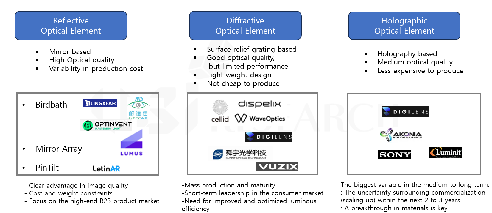
Figure 1. Comparison of AR optical system architectures and major suppliers. Source: UBI Research
| Structure | Strengths | Key Constraints | Target Market |
|---|---|---|---|
| Prism / Freeform | Easy quality control | Size & weight limits | Industrial & Medical |
| Birdbath | Mature ecosystem, high quality | Bulky, obstructed external vision, discomfort during longer wear | Watching Videos· Personal Entertainment |
| Geometric waveguide | Potential for Luminous Efficiency and Color uniformity | Precision stacking, process complexity, yield | Premium B2B AR |
| Diffractive waveguide | Compact and Lightweight, Scalability of the Process | Luminous efficiency, rainbow effect, color uniformity | Daily Wear and the Mass Consumer Market |
| VHG / PVG | Thin structure and flexibility in optical design | Material Properties and Process Stability | Mid- to Long-Term Consumer and Specialty Products |
Table 1. Comparison of the Advantages and Disadvantages of AR Optical Systems by Type
The waveguide approach confines the optical path within a thin lens substrate, allowing for a design that closely resembles ordinary eyeglasses. Since users view the outside world through a transparent substrate rather than a complex translucent optical block, a high see-through transmittance can be achieved. Using a high-refractive-index substrate broadens the range of angles at which total internal reflection is possible, enabling a large field of view (FOV) with a single lens; furthermore, when the optical structure and materials are optimized, brightness attenuation and chromatic aberration at the edges of the field of view can be reduced. These advantages are not independent of one another. Expanding the FOV makes it difficult to ensure optical efficiency and color uniformity, while widening the eyebox increases light distribution loss. Therefore, the key to waveguide technology lies not in achieving a single optimal specification, but in simultaneously balancing the FOV, efficiency, eyebox, transmittance, and uniformity within the target product’s weight and power consumption constraints.
A geometric reflective waveguide guides light beams using the principles of geometric reflection by precisely stacking an array of ultra-small partial reflection mirrors within a glass substrate. Lumus’s ZOE technology achieves a field of view (FOV) of approximately 70 degrees, and the luminous efficiency of the geometric reflective combiner ranges from 600 to 1,000 nits/lm. It offers a distinct advantage in image quality by reducing rainbow effects and chromatic aberration caused by diffraction. On the other hand, the alignment of the mirror array and the stacking and bonding processes are challenging, resulting in high manufacturing costs and yield issues. The arrayed reflective mirrors may appear as faint diagonal lines from the outside, and there are limitations to reducing the product’s weight and cost. Therefore, it is highly competitive in industrial, medical, and high-end B2B markets that prioritize high image quality and functionality, while expansion into the mass consumer market depends on process automation and yield improvements.
A diffractive waveguide diffracts light and guides it to the eye by forming a surface-relief grating—a nano-scale pattern of ridges and grooves—on the substrate surface. Its advantages include a thin and lightweight form factor and nanoimprint-based mass production. The optical efficiency of the combiner ranges from 50 to 400 nit/lm, with a typical field of view (FOV) of 50 to 55 degrees; some designs extend this up to 70 degrees. With its high process scalability, this is the technology closest to being adopted for daily wear and the mass consumer market. Key limitations include low luminous efficiency, rainbow effects, light leakage, and color fringing. Performance is determined by the precision of grating fabrication and the optical properties of high-refractive-index resins; low luminous efficiency increases the power consumption required to drive the microdisplay and the thermal design burden to achieve the same eye brightness. While SRG offers the highest mass-production potential, it is difficult to completely eliminate color fringing. While VHG and PVG can theoretically achieve higher light efficiency, many products are limited to a field of view (FOV) of 30–40 degrees due to the refractive index range of the photosensitive materials. Future improvements in the refractive index modulation range of the materials, environmental stability, and large-area uniformity will determine the pace of commercialization.
| Item | Geometric Reflective Waveguide | Diffractive Waveguide |
|---|---|---|
| FOV | ~ 70° (Lumus ZOE technology) | 50~55° (Max 70°) |
| Wight | 11~14.5 g (Lumus Z-30 optical engine product) | 4~8g (all-resin waveguide) |
| Luminous efficiency (Combiner) | 600~1,000 nit/lm | 50~400 nit/lm |
| Color Performance | Almost no color dispersion | Rainbow effects and color uniformity issues |
| Key Challenges | Complicated processes and yield | combiner Efficiency, FOV |
Table 2. Comparison of geometric reflective waveguides and diffractive waveguides..
SiC has a refractive index exceeding 2.6 and a high thermal conductivity of approximately 120–490 W/m·K. The high refractive index broadens the range of angles at which total internal reflection can occur within the substrate, enabling the field of view (FOV) of a single-layer waveguide to be expanded to over 70 degrees, while the high thermal conductivity increases the potential for simplifying the heat dissipation structures of projectors and optical modules. Furthermore, the increased design freedom in diffraction allows for the reduction of rainbow effects and color fringes, while improving brightness and color uniformity across the entire field of view.
Meta Orion achieved a field of view of approximately 70 degrees by applying SiC lenses and complex nanoscale waveguide structures. This serves as a real-world example demonstrating SiC’s potential for large fields of view in actual systems. However, SiC wafers are expensive, and managing defects, performing nanoscale etching, ensuring surface quality, and conducting inspections are costly and technically challenging. While Chinese companies are leading the development of products that combine SiC etching and NIL, their entry into the mass consumer market depends on improvements in material costs, etching yield, and large-area uniformity.
| Evaluation Item | Key Checkpoints | Business Impact |
|---|---|---|
| Material | Wafer size, defect density, thickness/refractive index uniformity | Raw material cost & effective area |
| Processing | Etching depth/angle uniformity, surface roughness | Optical efficiency, color uniformity, yield |
| Optical Performance | FOV, eyebox, MTF, stray light, rainbow effect | User experience & microdisplay power |
| Reliability | Stability after temp., humidity, and shock exposure | Customer qualification period |
| Manufacturability | Cycle time, inspection takt time, reworkability | Good die cost & supply capacity |
Chinese manufacturers use glass, resin, and SiC in parallel because no single material can meet all product applications. For Daily Wear, cost and lightweight design are priorities, so improvements in glass- or resin-based replication processes are critical. For True AR, the need for SiC and high-refractive-index glass is relatively higher due to the requirements for a wide field of view (FOV) and high performance. The performance of diffractive light guides is determined by high-refractive-index materials, grating machining precision, and nanoimprint replication quality. While SiC is advantageous for expanding the FOV, it is costly and difficult to etch. Therefore, the development direction of Chinese companies should be viewed not in terms of the relative merits of specific materials, but rather in terms of how they balance the target FOV, weight, optical efficiency, color performance, and mass production difficulty.
The superiority of a waveguide is not determined by a single specification. Products for daily wear, True AR, sports, and industrial and medical applications have different objectives in terms of field of view (FOV), eyebox, wearability, and reliability. If a supplier attempts to apply the same product to all markets, there is a high likelihood of either over-specification or excessive costs.
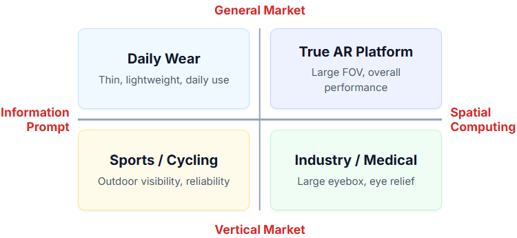
Figure 2. Market positioning of the AR waveguide product line.
| Product Category | Priority Metrics | Suitable Development Direction |
|---|---|---|
| Daily Wear | Weight, thickness, power, cost | Medium FOV, thin lens, proven replication |
| True AR Platform | Large FOV, color uniformity, eyebox | SiC / high-index material, premium optics |
| Sports / Cycling | Outdoor visibility, clear view, safety | Info-display, high brightness, rugged |
| Industry / Medical | Long eye relief, wide eyebox, reliability | Custom design, certified long-term stability |
At the CIOE 2026 exhibition, products featuring diversified materials and processes—with a focus on diffractive types—were on display. The information below is based on the exhibited products, company descriptions, and forum presentations; the numerical specifications are values provided by the companies at the time of the exhibition and do not represent the results of independent tests conducted under identical conditions.
| Company | Identified Tech Trends | Business Implications |
|---|---|---|
| Goeroptics | Diffractive waveguides (Glass/Resin/SiC). Glass etching, nanoimprint, & SiC etching. | High customization via broad material/process options. Mass production yield comparison required. |
| SEEV | SiC etching & NIL diffractive waveguides. 20–30° FOV custom & full-color displays. | Must benchmark SiC FOV, color uniformity, and cost against glass alternatives. |
| Luxshare | Holographic waveguides (HOE/PVG) integrated with microdisplays. | Shifting from components to modules. Finished product optical/assembly yield is critical. |
| Nikahood | VHG single-layer structures. Ranging from mono-green to full-color. | Commercialization depends on balancing thinness with material & environmental reliability. |
| Greatar | Grating design & nanoimprint mass production. Expanding to resin, high-index glass, & SiC. | Material diversification leveraging NIL expertise. Monitor future parallel use of etching processes. |
In the short term, daily wear, sports, and industrial products are most likely to drive actual shipments. In this market, cost, weight, power consumption, and stable yield are more important than maximum field of view (FOV). Therefore, it is necessary to prioritize tracking the pace of improvements in glass- and resin-based diffractive waveguides and the NIL process.
In the medium- to long-term True AR market, SiC, VHG, and PVG are candidates for performance expansion. SiC has great potential in terms of a field of view (FOV) exceeding 70 degrees and thermal management, but it is characterized by high material costs and processing difficulty. VHG and PVG offer potential for improved light efficiency, but challenges related to the refractive index of photoresist materials and FOV limitations must be addressed.
Consequently, it is more likely that waveguide technology will evolve in parallel according to specific product requirements rather than having a single approach replace the entire market. The technological competitiveness of Chinese companies will depend on how quickly they can achieve a balance between FOV, weight, light efficiency, color uniformity, and mass-producibility by combining glass, resin, and SiC with etching and nanoimprint processes.
UBI Research, CIOE 2026 On-Site Survey and Exhibition Product Data, September 2026.
Meta, “Introducing Orion, Our First True Augmented Reality Glasses,” September 2024.
CIOE, AR/VR Exhibition Section and Official Materials for the 2026 Event.