
1. IT OLED Market Outlook and Gen 8.6 Investment Trends
IT OLED shipments are forecast at 31.8 million in 2026 and 58.6 million in 2030. Tablets rise from 14.3 million to 23.4 million; notebooks, 12.5 million to 19.5 million. Monitors show the largest gain, from 5.0 million to 15.7 million, lifting their share from about 16% to 27%.
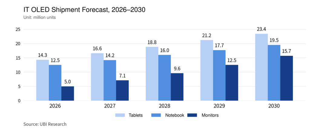
IT OLED Shipment Forecast by Product, 2026–2030
Gen 8.6 Investments and Processes
| Panel Maker and Line | Patterning and TFT | Key Milestones | Capacity (sheets/mo.) |
Investment |
| Samsung Disp. Asan A6 |
FMM deposition Oxide TFT |
Jul 2026 Mass production starts |
15,000 sheets | KRW 4.1 tn |
| BOE Chengdu B16 |
FMM deposition LTPO/LTPS TFT |
Jun 2026 Mass prod. and first delivery |
32,000 sheets | CNY 63 bn |
| Visionox Hefei V5 |
Photo patterning ViP |
Equip. move-in: Apr 2026 Mass prod. target: 2027 |
32,000 sheets | CNY 55 bn |
| TCL CSOT Guangzhou T8 |
Inkjet printing IJP |
Frame complete: May 2026 Mass prod. target: Q4 2027 |
22,500 sheets | CNY 29.5 bn |
Capacity: planned motherglass input. Investment: project announcements. [1–10]
LG Display has yet to invest in a new Gen 8.6 IT OLED line but is validating photolithographic OLED processes using existing Gen 8.5 white OLED equipment.[11]
This report focuses on photolithographic OLED, which patterns IT OLED pixels without FMMs. It compares pixel formation and device protection at LG Display, Samsung Display, and Visionox, and examines each technology’s features and adoption challenges.
Sources [1] Samsung mass-production announcement / [2] Visionox V5 announcement / [3] BOE mass-production announcement / [4] TCL T8 announcement / [5] TCL half-year report / [6] Samsung investment announcement / [7] Samsung planned capacity / [8] BOE investment and capacity / [9] V5 mass-production target / [10] BOE TFT configuration / [11] LG technology seminar
2. Characteristics and Evolution of Photolithographic OLED
■ Transition from FMM to Photo Patterning and Process Challenges
FMM evaporates organics through fine mask openings to form RGB pixels. Photolithographic OLED defines pixel boundaries by exposure and development, easing metal-mask sagging and alignment constraints. Etching unwanted films or lifting them off with temporary patterns exposes organics to chemicals or plasma. Encapsulation is thus needed during patterning to protect pixels, ensure precision, and preserve existing device properties.
■ Applied Materials’ Pixel Structure and JDI’s Panel Implementation
Replacing FMM requires pixel patterning, device protection and electrode connections. Applied Materials’ patents and JDI’s eLEAP illustrate process structures and actual panels, respectively, providing the technical basis for the three panel makers’ photolithographic OLED below.
Applied Materials’ US11476313B2 (priority: September 2020) uses protruding overhangs to separate deposited films and per-pixel encapsulation to protect organics. Cathodes contact conductive portions below the overhangs.[12] Its MAX OLED, announced in 2024, integrates deposition and encapsulation. At SID 2025, it showed how deposition-angle control makes cathodes wider than organic layers to ensure contact.[13,14]
JDI’s photolithographic OLED eLEAP, announced in 2022, combines FMM-free evaporation and photolithography with high-mobility oxide TFTs, achieving a 60% aperture ratio at 300 ppi. JDI also outlined its use on Gen 8 and larger substrates.[15]
■ Photolithographic OLED Prototypes for IT Applications
LG Display’s 27-inch FLiPP (FMM-Less innovative Pixel Patterning), unveiled in 2026, demonstrates monitor-size photolithographic OLED.[16] At SID 2026, Visionox showed a 16-inch-class ViP notebook panel with a tandem stack of two or more emissive units.
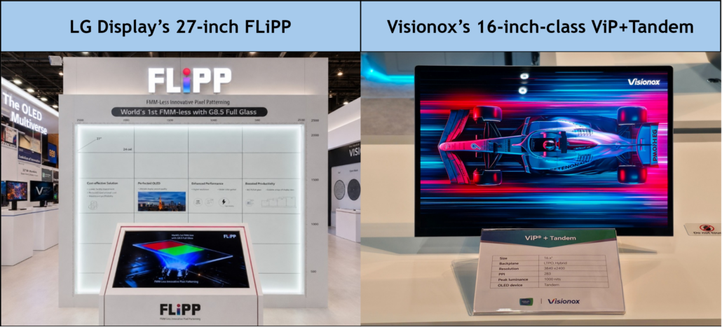
Figures 2 and 3 Photolithographic OLED Exhibits from LG Display and Visionox
Sources [12] US11476313B2 / [13] MAX OLED announcement / [14] SID 2025 paper / [15] JDI eLEAP announcement / [16] FLiPP exhibit and investment review article
3. Processes and Development Status by Company
3.1 Sequential Patterning and Auxiliary Electrodes in FLiPP
LG Display is developing FLiPP for initial use in tablets and notebooks. It is considering adding exposure equipment to its existing Gen 8.5 white OLED facilities and modifying oblique deposition sources to establish cathode contact.[11,16]
Patent US20250212619A1 exposes only the target color’s anode, then forms the organic layer, cathode, and encapsulation in sequence before proceeding to the next color. Overhangs separate deposited films between pixels, while auxiliary electrodes connect the color-specific cathodes.[17] Figure 4 shows the FLiPP process using molybdenum (Mo) auxiliary electrodes, silicon oxide (SiOx) or silicon nitride (SiNx) pattern layers, and amorphous silicon (a-Si) overhang caps. Encapsulation protects completed pixels while the remaining colors are patterned.
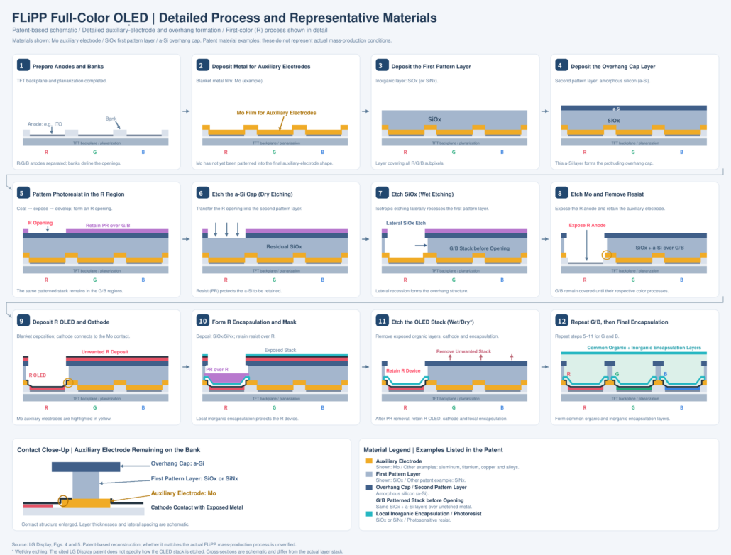
Figure 4 FLiPP Process Diagram Based on Related Patents
Sources [11] LG Display technology seminar / [16] Review of using existing facilities for FLiPP / [17] LG Display US20250212619A1
3.2 MPO Lift-Off and Acquisition of Orthogonal Patents
Samsung Display is developing a 7-inch-class MPO (Micro Patterned OLED) prototype. Development began in March 2026, with samples planned for year-end.[18] In the related patents, lift-off removes films on a temporary pattern together with the sacrificial layer, leaving the pixels.
Samsung Display bought five U.S. FMM-free OLED patents from Orthogonal in 2024.[19,20] Samsung-filed US10243175B2 covers lift-off using a fluorinated sacrificial layer and HFE (hydrofluoroether) solvent, while US11925071B2 protects the emissive layer during this process.[21,22] Reconstructed from related patents, the MPO process in Figure 5 forms a common cathode after RGB patterning.[19,21]
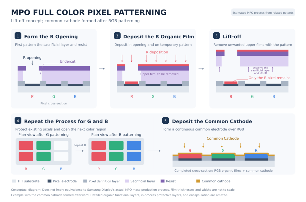
Figure 5 MPO Lift-Off Process Diagram Based on Related Patents
Lift-off must selectively dissolve the sacrificial layer without damaging organic layers or their interfaces. Lift-off residue and pixel-edge damage require care, as they can cause defects in the common cathode formed afterward.
Sources [18] Report on MPO development / [19] US10468637B2 and assignment history / [20] Report on the Orthogonal patent acquisition / [21] US10243175B2 / [22] US11925071B2
3.3 ViP’s Insulating Isolation Structure and Metal Conductive Portion
Visionox supplies products for Honor wearables from its Gen 6 ViP line and is applying ViP to the new Gen 8.6 V5 line.[2] US20240251605A1, in the same family as CN115224222B, separates films with a SiNx or SiOx isolation structure and connects cathodes through separate metal conductive portions. The pixel-defining layer (PDL) covers anode edges to prevent shorts with the conductive portions.[23]
This structure wet-etches metal to leave conductive portions beneath insulating caps.[23] Figure 6 combines this with the color-specific encapsulation and unwanted-stack removal in US20260040765A1 to illustrate the ViP process.[24]
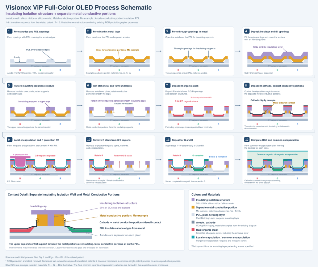
Figure 6 ViP Process with Insulating Isolation Structures and Separate Metal Conductive Portions
Thicker films in tandem structures can make patterning harder to control than in single-stack structures. Cathode contact and sidewall encapsulation must be secured while suppressing film bridging beneath isolation structures and etch residues.
Sources [2] Visionox V5 equipment move-in / [23] CN115224222B / Same patent family: US20240251605A1 / [24] US20260040765A1 / [25] CN118785759A
4. Key Differences among the Three Technologies
The three technologies differ in pixel isolation structures and cathode formation sequence. The table compares the main differences in the patents and process diagrams above.
| Item | FLiPP | MPO | ViP |
| Pixel isolation | Overhang | Temporary-pattern lift-off | Insulating isolation structure and cap |
| Key materials | Mo auxiliary electrode SiOx/SiNx and a-Si |
Fluorinated sacrificial layer and lift-off solvent |
SiNx or SiOx isolation Metal conductor, e.g., Mo |
| Excess film removal | Stack etching Wet or dry (patent silent) |
Lift off sacrificial layer with overlying films |
Wet etching of stacks (Patent example; dry etching possible in practice) |
| Cathode connection | Each color’s cathode contacts auxiliary electrode |
After RGB patterning, form a common cathode |
Per-color cathodes join separate conductors |
| Key controls | Etch damage; cathode contact and encapsulation |
Solvent compatibility Lift-off residue; pixel edges |
Conductor etch/contact Insulation / sidewall encapsulation |
Sources [14] SID 2025 paper / [17] LG Display US20250212619A1 / [19] US10468637B2 / [21] US10243175B2 / [23] CN115224222B / [24] US20260040765A1
5. Performance Improvements and Application Challenges
LG Display said FLiPP raised aperture ratio from conventional FMM’s 42% to 65%. At equal luminance and luminous efficiency, current density per emitting area is calculated at about 0.65 times the original level. LG Display said this gain can deliver 1.6 times the luminance, 2.4 times the lifetime, or 13% less power. Higher aperture ratio is a shared benefit of photolithographic OLED, which avoids FMM sagging and alignment limits; MPO and ViP can thus expect similar performance gains.
Large-area mass production requires uniform enlarged emitting areas across the substrate. FMM sagging and alignment constraints ease, but exposure, etching or lift-off defects, electrode contact, and encapsulation quality affect yield. Added steps’ impact on total production time also needs assessment.
FLiPP forms and encapsulates each color’s organic layer and cathode, then repeats patterning. Earlier pixels must be protected from later etching, with contact secured between each cathode and the auxiliary electrode. MPO forms a common cathode after RGB patterning, so emissive-layer damage and residue during sacrificial-layer lift-off must be reduced. For the metal isolation structure in ViP-related patents, the etched conductive portion’s shape and pixel-sidewall encapsulation are critical. Thicker tandem stacks can make this shape control harder.
The three technologies’ competitiveness ultimately hinges on converting aperture-ratio gains into yield and productivity on large-area substrates.